


Building Board-Level Assemblies for LED Modules
Introduction
Light emitting diodes (LEDs) are quickly becoming the lighting solution of choice. Key benefits include significantly better efficiencies and lifetimes than incandescent, halogen, and even compact fluorescent (CFL) bulbs. LEDs are also compact, robust, high brightness, and available in a range of output wavelengths, plus white light in various color temperatures. As a result, their applications go beyond general lighting. They’re also widely integrated into products for the automotive, aviation, gaming, healthcare, horticultural, and industrial markets, to name a few. It’s not enough to buy a high-quality device, though. Getting the expected lifetime and performance from LEDs requires informed design and effective integration into the printed circuit board (PCB). Here, we talk about key factors in the board-level assembly of LED modules, including how to specify the design, integration considerations, and best practices to ensure optimal results.
Applications of LEDs
LEDs are ubiquitous in the modern world. Applications include:
- General lighting
- Functional illumination, e.g., lighting keyboards, back lighting displays, and illuminating instruments
- Indication lighting, e.g., status lighting on electronics, etc.
- Aesthetic lighting, e.g., architectural accent lighting, wash lighting, etc.
- Sensors, e.g., motion detectors, presence/absence sensors, remote control IR emitters and receivers, etc.
- Flat-panel displays
- Photosensitive materials curing, cleaning, disinfecting, and sanitizing

Understanding LEDs
Light generation
LEDs are direct-bandgap semiconductor devices that generate optical output through the mechanism of electroluminescence. The devices are based on p-n junctions, where a p-type region (excess positive charges) contacts an n-type region (excess negative charges; see Figure 1). Without an applied voltage, a depletion region forms between the two, acting as an insulator to prevent electron flow. If the LED is forward biased, the voltage energizes the free electrons in the n-type region so that they cross the depletion zone to recombine with the holes in the p-type region. When the charges recombine, the material emits a photon with an energy (and wavelength) determined by the bandgap – charge difference – of the material. This process takes place spontaneously as soon as voltage is applied.
LED materials have been developed that generate output across the entire optical portion of the electromagnetic spectrum, from far infrared (IR) to ultraviolet (UV) wavelengths. LEDs also can produce white light through color mixing. The most common approach is to excite a yellow phosphor with a blue LED, although white-light LEDs based on RGB triads are also available.

Figure 1: Electroluminescence occurs at a p-n junction when a negative charge (an electron) crosses from the n-type region to recombine with a positive charge (a hole) in the p-type region. (Source: S-kei, Wikimedia Commons)
Because LEDs are diodes, they can only pass current when forward biased. If reverse biased, they will block the current. For a device to generate output, the applied voltage must exceed threshold. Output brightness is proportional to drive current – to a point. In general, increasing drive current will increase output, until levels reach the breakdown point, burning out the device. To prevent this, an LED should be wired in series with an appropriately sized breakdown resistor or other current-limiting control device.
Mounting styles
LEDs are available in two mounting styles: through-hole devices and surface-mount devices (SMDs), which are designed for use with surface-mount technology (SMT) assembly techniques (more on that later).
Through-hole LEDs
In a through-hole LED, the emitter chip and its contacts are encapsulated in an epoxy-resin case. Two or more connector pins project from the case for connecting the device to a voltage source (see Figure 2).

Figure 2: In through-hole LEDs, the emitter chip and contacts are enclosed in an epoxy-resin case, with the connector pins projecting. [Source: American Bright website]
Through-hole LEDs are attached to the circuit board by feeding the pins through holes drilled in the PCB and soldering them on the back side. The mechanical connection increases the strength of the bond, which is beneficial for high shock and vibration environments such as found in certain industrial, automotive, and even aviation applications. On the downside, through-hole LEDs involve additional assembly steps and frequently require manual installation, making the assembly both more time-consuming and expensive. Human factors also reduce yield.
SMD LEDs
In an SMD LED, the emitter chip and circuitry are mounted in a flat-bottomed package with conductive pads underneath or on the edges (see Figure 3). The design eliminates the need for drilling holes and manual placement. Instead, SMD LEDs can be attached to the board using high-speed pick-and-place equipment and reflow soldering.

Figure 3: SMT LED edge options include (clockwise from top right) yoke, z profile, gullwing, and straight. [Source: American Bright website]
There are four common package types:
- SMT chip packages: Surface-mount LEDs are cost-efficient solutions for low-power, compact designs. They are also lighter weight than other packaged LEDs.
- Plastic-leaded chip carrier packages (PLCC): Optimized for mid-power LEDs, PLCC packages enable the devices to either be attached directly to the board or mounted in a socket that is soldered to the board. In the latter case, the LED on the finished device can be removed and replaced in the field.
- Epoxy molding compound (EMC) plastic packages: EMC packaging is increasingly used for high-power LEDs because of its ability to withstand higher temperatures without discoloration. In addition to EMC, other plastics used for this type of packaging include polycyclohexylenedimethylene terephthalate (PCT), polyphthalamide (PPA), and silicone composites.
- Ceramic or metal-lined ceramic pedestals: Ceramic packages are soldered directly to the board and are best for higher powered LEDs.

Figure 4: SMTs – Top Emitting (left) and Side Emitting (right)
Chip on Board (COB) LEDs
COB LEDs are mounted directly to the board, without any additional packaging. The approach supports extremely high device densities, and, thus, high luminous flux density. COB LEDs make it possible to create a uniformly distributed light surface that generates soft light with less glare.
At present, the technology is widely used in bulbs, spotlights, downlights, streetlamps, industrial and mining lamps, and other types of fixtures.
Benefits of LEDs
- Long lifetimes: LEDs can be operationally effective for as much as 100,000 hours. The extended lifetimes reduce maintenance and provide the support necessary for high-reliability applications. It’s important to note that LEDs don’t fail catastrophically. Instead, their output gradually dims over time.
- High-efficiency: As solid-state devices, LEDs have high electrical-to-optical conversion efficiencies. The reduction in power consumption, coupled with the extended lifetime, significantly reduces operating expenses. This leads to lower total cost of ownership, despite the slightly higher purchase price.
- Small size: LEDs are compact devices ranging from millimeters to microns in diameter. They make excellent solutions for space-constrained applications or devices with unique form factors.
- Flexibility: LEDs provide OEMs with a great deal of design freedom. They can be assembled in a variety of configurations to meet the needs of the application, whether on PCBs, light strips, or custom substrates. They’re available in multicolored devices that can be programmed to cover the full color gamut. Because brightness is a function of drive current, lighting levels can be easily adjusted.
- Reliability: LEDs do not have glass envelopes or fragile filaments subject to breakage. They can tolerate large amounts of shock and vibration.
- High color rendering index (CRI): Expressed on a scale from 0 to 100, CRI is a metric for how close the colors of objects illuminated by the source match those of objects illuminated by the sun. High-quality white light LEDs have CRIs in the high 90s.
- Broad color range: LEDs are available with output from the IR to the UV spectral regions. In the case of white-light LEDs, a variety of phosphors have been developed to produce a range of correlated color temperatures (CCTs), from cool white to warm white.
- Environmentally friendly: LEDs are lead free, making them compliant with the Restriction of Hazardous Substances Directive (RoHS). The increased efficiency and lifetime lower energy and resource consumption, enabling owners to reduce their carbon footprints.
Key markets
LEDs have made deep inroads into the general lighting space. In addition, they have significant market share in a range of sectors:

Architectural lighting
LEDs, particularly flexible LED solutions, are widely used for architectural accent lighting, both indoors and outside. The extended lifetime, ease of installation, and range of colors gives lighting designers the ability to create a variety of effects in almost any structure.

Automotive
The core benefits of high efficiency, long lifetime, small size, and light weight make LEDs ideal for vehicles ranging from passenger cars to trucks and buses. They are used for passenger compartment lighting, instrument illumination, signaling, headlights and taillights, and more. Because of the need to ensure user safety, facilities manufacturing automotive LEDs and LED modules should have specialty automotive manufacturing certifications like AEC Q101 and AEC Q102.

Aviation
LEDs have become common in aircraft cabin lighting. The broad color gamut and programmability provided by LEDs enable airlines to give passengers a sophisticated and memorable experience, while the efficiency and long lifetimes reduce operating costs. LEDs are also effective for indication lighting and functional illumination such as instrument backlighting and display lighting. For best results, LEDs and LED modules for aircraft applications should be manufactured in an AS9100-certified facility (see below).

Entertainment
Cost efficient and reliable, LEDs are applied throughout the entertainment industry, for general lighting, accent lighting, functional illumination, and indication lighting. LEDs add flash and color to slot machines and excitement to casinos via accent lighting. They enable the Jumbotrons that have become an expected part of the experience in stadiums and arenas.

Horticultural lighting
Processes like photosynthesis and foliage growth can be optimized using very specific wavelengths. With the ability to provide color-tuned illumination, LEDs play an increasingly important role in horticulture. Once again, efficiency and long lifetime make them cost-effective alternatives to traditional grow lights. Users can take advantage of easy-to-deploy strip lighting with IP68 ratings to protect against contamination.

Industrial
LEDs are indispensable in the modern industrial environment. They’re fundamental to the highly engineered light sources required for machine vision. They illuminate the human-machine interfaces (HMIs) used to run equipment and in the indication lights that display status on a host of devices. They’re also effective for general lighting. Depending on application and environment, modules need IP ratings to protect against contamination.

Medical
LEDs provide general lighting in operating rooms, patient rooms, and public spaces. They’re widely used in medical equipment, from infusion pumps to UV curing wands. The reliability, long lifetimes, and low maintenance and power consumption make them ideal for these mission-critical yet cost-sensitive applications.

Appliances
Whether for appliances, home electronics, or sensors, LEDs have become increasingly popular light sources for consumer OEMs. Applications range from illumination to indication to display backlighting. The compact form factors suits space-constrained designs, while high efficiencies and long lifetimes help manufacturers field cost-competitive products.
No matter the market, OEMs and integrators are better served focusing their limited engineering resources on market differentiators rather than on the complexities of LED modules. Fortunately, the LEDs industry has stepped up with solutions. OEMs can work with vertically integrated suppliers that provide LEDs packaged with integrated IC drivers and breakdown resistors, or even fully assembled LED lighting modules (see Figure 4).
LED PCBs
Any discussion of LED board-level assembly needs to start with the PCB. The specific characteristics and requirements of LEDs and their applications have led to the emergence of a class of boards called LED PCBs. Before we go into further detail, let’s start with some background.
Circuit board basics
A simple PCB consists of a dielectric substrate, also known as a laminate, overlaid with a copper foil that is a few tens of micrometers thick (see Figure 5). The copper foil is etched to form conductors, or traces, to connect the components. After patterning, the copper will be covered by a finish coat to prevent oxidation. The components are then soldered onto the board, either by using predrilled holes, as for through-hole LEDs, or onto pads, as for SMD LEDs. When the LED module is complete, it just needs to be connected to power in order to operate.

Figure 5: A single-sided PCB consists of a dielectric substrate topped by a patterned copper foil, topped by selectively deposited solder to attach components. [Source: American Bright website]
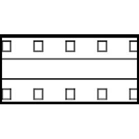
Single-sided PCBs do have some drawbacks. They have limited board space and only support a single voltage. Double-sided PCBs feature copper on both sides of the dielectric substrate, doubling board space and voltage options (see Figure 6). On the downside, they are more expensive and more difficult to fabricate and work with.

Figure 6: Double-sided PCBs have copper traces on both sides of the substrate. Vias/PTHs can be used to connect circuits on different sides of the board or for heat transfer.
Metal-core PCBs – LED PCBs
As efficient as LEDs are, each individual device only produces a limited amount of output. This might be sufficient for a sensor or simple indication light such as a circuit board status light. Many applications, particularly in general lighting and accent lighting, require more LEDs to generate sufficient lumens. As a result, a single LED board may hold dozens of LEDs. This presents a significant challenge.
Although LEDs do not radiate heat from the front side in the same way as incandescent bulbs, they do generate a significant amount of heat off the back side. Elevated temperatures are problematic for electronics, and LEDs are no exception. Operating an LED above its rated temperature can reduce lifetime and cause wavelength drift. As a result, thermal management is a key aspect of the design phase, and of PCB specification, in particular.
The standard dielectric substrates used for most LEDs have low thermal conductivity. Typically, plated through holes (PTHs) on the PCB are used to draw heat away from the copper layers. In the case of a board with only one or two LEDs, this may be enough. PCBs with a large number of LEDs require more effective heat dissipation, however. The solution is to use metal-core PCBs.
In a metal-core PCB, the standard dielectric substrate is replaced by a metal substrate separated from the copper layer by a thermally conductive dielectric adhesive (see Figure 7). Heat passes through the adhesive to the metal layer, where it is dissipated.

Figure 7: In a metal-core PCB, a thermally conductive dielectric adhesive transfers heat from the copper layer to a metallic substrate, where it is dissipated. [Source: American Bright website]
A variety of metals can be used in metal-core PCBs, including copper, aluminum, and various alloys. Copper has significantly higher thermal conductivity than aluminum, but it’s also heavier and more expensive. Most LED PCBs use aluminum for the substrate, which also adds mechanical strength. They may include an aluminum alloy coating on the bottom to protect against oxidation and scratches. LED PCBs can be fabricated in double-sided versions, although the configuration reduces their heat dissipation capabilities.
LED printed circuit-board assembly (PCBA)
For decades, PCB assemblies were manufactured by manually inserting the leads of through-hole components through predrilled holes in the PCB and soldering them in place on the back side. The process worked but it was time-consuming, difficult to automate, prone to error, and expensive. SMT was developed in the 1960s as an alternative.
SMT is a highly automated method for mounting components to the surface of a PCB with great precision and reliability. SMT technology offers many advantages over through-hole technology, including increased component density, superb signal integrity, shorter assembly time, reduced labor costs, higher yields, and better operational flexibility, to name a few. As an example, the SMT process can be used to place components as small as 0.25mm X 0.125mm (the 0201 package) at a rate of 20K pieces per hour using a single pick-and-place station.
There is still a need for through-hole devices – and the associated processing steps – on almost all PCB assemblies. Even taking this into account, SMT has become the primary method for assembling electronic products.
The SMT line
The process of LED PCB assembly starts with inspection and service preparation of the PCB. Next, the boards go through the SMT line, which consists of several discrete steps:
Solder paste printing
SMTs are attached to the PCB using a method called reflow soldering, which uses a solder paste consisting of a mixture of powdered solder and flux. The choice of materials varies depending upon the devices, the board, and the application.
For years, tin-lead solder was the industry standard, but the passage of RoHS and other directives has pushed the industry toward lead-free alloys based on tin. Commonly used lead-free solders include tin-copper-nickel alloys and tin-silver-copper alloys, available in a vast variety of compositions. Trace elements are used to modify properties for various applications.
The first step in SMT processing is to apply the solder paste to the surface of the PCB (or a panel of PCB matrix) prior to the placement of electronic components. In solder-paste printing, a precise amount of solder paste is forced through openings in a stencil designed to coat specific pads on the PCB. After the solder paste is transferred to the PCB, the board moves to the pick-and-place station for component placement.
Solder printing is one of the critical steps that influences the overall efficiency and yield rate of the PCBA processes. The diameter of the solder beads and the viscosity of the mixture need to be tailored to the stencil, and the particulars of the components and the application. Consistency of solder printing, particularly the amount of paste, paste condition, and printing precision, dictates the limitation and boundary of PCBA layouts, i.e., the number of components can be accommodated on a PCB.
Automated inspection devices are required to optimize solder printing, particularly for mass production of high-density LED PCBs. For example, automated optical inspection (AOI) with AI image analysis can quickly pick up defects such as solder bridging, uneven pasting, misalignment, and insufficient/excessive deposition. We’ll discuss this in further detail below.
SMT placement
The core units of an SMT system are stations equipped with sophisticated pick-and-place machines for placing the components on the proper pads. The solder paste is tacky enough to hold the devices in place while the board moves through pick-and-place in inspection, then passes to the reflow oven.
Multiple pick-and-place stations can be arranged in a variety of sequences that suit different types and sizes of SMT components, to speed optimization and improve first-run yield. An SMT line can be flexibly arranged and integrated to fit a wide range of automated assembly needs. This integration lowers production costs by increasing output and reducing defects.
Reflow ovens
A production-scale reflow oven is a tunnel oven with a number of thermal zones for tightly controlled heating and cooling (see Figure 8). The oven is used for melting solder paste (“solder reflow”) and forming solder joints between the electronic components and the PCB. The structure of multiple thermal zones is designed to ensure that the solder paste melts evenly and precisely at specific temperatures defined by the recommended soldering curve.

Figure 8: Reflow soldering process profiles give detailed time/duration directions for (from left) preheat, operating heat, and cooling. [Source: Wikipedia]
It should be noted that the soldering curve varies with the type and composition of the solder paste. The temperature setting of each thermal zone should also be adjusted to account for the types and sizes of PCBs and the loading rate. In the case of LEDs, which are encapsulated in various types of polymers and resins, the solder process profile must be compatible with that of the device or it may cause damage to the packaging.
When the solder paste melts and solidifies, the SMT components are bonded to the PCB permanently. In the case of double-sided PCBs, the boards are flipped and the sequence of printing-SMT-reflow repeats.
A variety of types of reflow ovens are available.
Through-Hole and Wave Soldering
SMT is not a universal solution, of course – it can only be used to process SMT components such as resistors, capacitors, diodes, transistors, and integrated circuits, however. Most PCBAs need at least some non-SMT components, such as electrolytic capacitors, inductors, coils, and connectors. After the board passes through the SMT line, the through-hole components must be installed.
Through-hole components can be attached to PCBs either by manual soldering or partially automated methods. In manual through-hole soldering, the leads are inserted into the PTHs in the PCB, bent at 90°, trimmed, and soldered. For soldering, the lead and pad are coated with flux, then heated to melt the solder and create mechanical and electrical connections. Excess solder can be removed by using a soldering wick or vacuum suction.
There are two soldering processes: dip soldering or wave soldering, both of which take place once the component leads have been threaded through the PTHs. In dip soldering, the entire board is dipped into the solder so that both leads and pads are coated. This is a semiautomated system that still requires some operator expertise. When the solder cools down and solidifies, all leads and pads are attached to form electrical joints.
Wave soldering, on the other hand, is a higher-speed, fully automated process that is far more eco-friendly. It involves preheating the PCB and components to activate the flux, and then passing the PCB assembly over a standing wave of molten solder. The wave of solder wets component leads and pads on the PCB. Once again, cooling creates a strong electrical and mechanical contact.
Through-hole soldering is often limited to small-scale production or repair work, as it is a manual process that requires skill and experience. Dip soldering and wave soldering, on the other hand, are more efficient and cost-effective processes that are suitable for high-volume production.
The choice of the soldering process depends on the specific requirements of the PCBA, manufacturing restrictions, scale of production, and yield-liability considerations. Through-hole soldering provides benefits for certain applications requiring higher level of mechanical durability and strength, while wave soldering is suitable for applications of high-speed, high-volume production.
SMT In-Line Inspection
SMT in-line inspection devices are specialized tools used at every step in the manufacturing of PCBs to ensure the proper placement of mounted components and soldering integrity. These devices are essential to identifying defects and rapidly detecting process abnormalities during each phase of the assembly operations. In-line inspection devices make it possible to reduce costly rework, down-time, scrap, and sales returns. In addition, these devices improve production efficiency and reduce the need for manual inspection and failure analysis. The result is significant improvement in quality, yield, and cost-effectiveness in modern LED PCB assembly.
A wide range of SMT in-line inspection devices are commercially available. In general, they can be categorized into four types:
Automated Optical Inspection (AOI): AOI uses cameras and software to capture and automatically analyze high-resolution images of PCBs for defects such as missing or misaligned components, excessive solder, and assembly anomalies. The software compares the images against a database of go/no-go benchmarks to determine whether a device is acceptable. Recent advances in the application of AI to machine vision have made AOI more capable and thorough.
X-ray Inspection: X-ray imaging makes it possible to detect internal defects such as voids in solder joints, misalignment, or solder bridging hidden underneath components. Similar to AOI systems, X-ray inspection systems can be operated in-line and continuously with proper software installed for automated image analysis and inspection.
In-Circuit Testing (ICT): ICT units use basic electrical testing to verify the connectivity and functionality of the components on PCBs. ICT units can be as simple as open/short testers, typically for detecting abnormalities of passive components. More advanced units evaluate active components such as transistors and integrated circuits. An ICT test fixture is connected to a computer that controls the test process. The computer sends signals to the PCB through the fixture, then measures the resulting signals to determine whether the circuit is functioning correctly. In-circuit testing is an efficient way of verifying the functionality and performance of both PCBs and PCBAs.
Functional Testing: A functional testing system is typically a simplified unit that evaluates the PCBA’s actions and responses under simulated conditions of use. Normally, a series of functional tests are conducted as part of system reliability “burn-in” and “start-up” verification. The functional burn-in test is normally conducted at 100% sampling rate for FQC.
Added to the continuous advancement of SMT technology, integration of in-line inspection devices in production lines significantly improves quality, yield, and cost-effectiveness in modern LED PCB assembly.
Challenges in LED PCB assembly
When it comes to LED modules, design is just the start. Board-level assembly of LEDs presents a number of challenges:
- Choice of PCB: The properties of the board can have a significant effect on coating, solder application, and device mounting. When defects arise, experience with a variety of boards makes it easier to determine a process-based solution.
- Proper spacing of devices: To enable successful assembly, different types of devices have recommended separations. This needs to be taken into account at the design stage. Experienced assembly teams can recognize these issues before manufacturing begins and suggest corrections or alternate solutions. Using an SMT LED with integrated driver and breakdown resistor, for example, can reduce the number of components on the board and lower device density.
- Choice of solder: Solder particle diameter needs to be matched to the scale of the stencil. Viscosity needs to be tailored to leave a pad of proper thickness and shape. The melting point of solder cannot exceed the temperature profile for the LED or damage can occur to the encapsulant or even the chip itself. Solders also need to be compatible with the end-use environment. Once at the factory, the solder needs to be properly stored and maintained; overly dry solder, for example, will lead to defects.
- Stenciling: Applying solder paste by stencil may seem like a straightforward step but there are many process parameters that can cause defects and reduce yield. These can range from seemingly simple parameters like squeegee pressure and speed to more nuanced issues like insufficient flux in the solder paste.
- Reflow: Reflow is another process that requires expertise. It is not enough to look at the thermal profile on the datasheet and set the reflow oven. Defects may uncover issues, whether it’s the wrong choice of solder, the need for a slower ramp rate, or a slight temperature adjustment for the actual reflow step.
- Test and inspection: Successful LED board assembly requires inspection and test at every point. In the case of LED modules, the testing process goes beyond verification of electrical properties. The LEDs need to be characterized to confirm operating wavelength and output. These tests require specialized equipment that may not be available in a standard board assembly facility.
- Depending on the application, manufacturing facilities may need to be certified to specific standards such as:
- AS9100: QMS for the aviation sector
- IATF16949: QMS for the automotive sectors
- ISO14001: Environmental management system (EMS)
- ISO 9001: QMS for manufacturing
Many of these standards go beyond simple product quality to require detailed risk management and supply-chain control. Maintaining certification requires ongoing commitment from the entire organization, enabling customers to identify suppliers they can trust.
Successful LED module assembly requires a deep understanding of a multitude of process variables and their effects on the end product. This is where subcontracting to an expert partner like American Bright comes in. We have specialty equipment and established processes that ensure every step of manufacturing, assembly, and test is done right – and we have the factory certifications to prove it. Our experienced engineers can look at board designs and bills of materials (BOMs) to identify issues and optimize performance and manufacturability. If a stock product will get the job done, we’ll find it. If a custom solution will be more effective, we can craft that, as well. Our skilled assembly technicians and test engineers have decades of experience manufacturing complex, high quality product, in volume. Leave the assembly to us so that you can concentrate on the elements that differentiate your product in the marketplace.
Conclusion
LEDs are swiftly becoming the dominant lighting technology. Building successful products for this market involves a number of variables. Fortunately, there are tools available to assist. LED PCBs are designed to dissipate the excess heat generated by high densities of LEDs. Integrated devices are designed for ease of assembly and deployment. Prebuilt LED modules are ready for use. Perhaps most important, manufacturing partners like American Bright offer the expertise gained from decades of LED board assemblies to perform this crucial but complex task reliably and economically.
Further reading
American Bright has more than 25 years of experience in board-level assembly of LED modules. Our factory certifications go beyond ISO-9001 to include AEC Q101, AEC Q102, AS9100, IATF16949, and ISO14001. Contact our experienced engineering staff to learn more about how we can help you get better product to market faster.